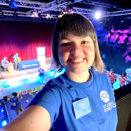
Vasiliki

Name: Vasiliki
Job Title: IC Engineer
Why did you choose a career in STEM?
I am lucky to come from a family that encouraged me to pursue a career in STEM as, ever since I was little, I loved maths, physics and computers and was always pulling things apart to try and figure out how they were made. It was no surprise that when it was time to select my university course, Engineering was my first choice. A career in STEM allows me to constantly learn and challenge myself while contributing to real-world advancements.
Your journey into Electronics
I discovered Electronics accidentally when my university offered a common first year for all engineering disciplines. I enjoyed all the mandatory Electronics modules so much that I switched my course to Electronic and Electrical Engineering and discovered the complex and challenging world of Electronics. Shortly after, I was encouraged to apply for a UKESF scholarship which gave me the opportunity to research the industry and understand the different paths that a degree in Electronics could take me, one of them being IC design. Three years later, I have successfully completed a 14-month placement with EnSilica as part of my UKESF scholarship, graduated from University and I am now working full-time as a Graduate IC Design Engineer. I am also actively promoting Electronics as a career path to younger people by visiting schools and participating in careers fairs, and trying to encourage more young women to pursue a STEM-related career.
What attracted you to EnSilica?
As a young female, getting started in the industry can feel intimidating. My colleagues at EnSilica immediately made me feel welcome and offered their full support throughout my placement, as well as during my final year at university and after my return as a graduate. During my placement, I have had the opportunity to join some very interesting and complex projects which significantly increased my skills and confidence and prepared me well for the remainder of my studies and for a career in the chip design industry. Additionally, I value the fact that I was encouraged by my managers to explore various aspects of IC design, such as digital, analogue, software or anything in between, equipping me with a unique combination of skills and knowledge.
What does an average day look like at work?
As an IC Engineer, no two days look the same. Every day is a chance to solve new design challenges and tackle problems that may arise. A typical day in the office starts at 9 am and includes a lot of problem-solving, researching improved design techniques, reading and understanding design specifications, learning to use new tools and exchanging ideas with colleagues. As part of a project team, you might be responsible for designing part of a chip, which usually involves writing the RTL in an HDL language such as SystemVerilog, and performing tests such as Clock Domain Crossing checks and Linting to optimise your design. As part of the design verification team, you will write testbenches and use more in-depth techniques such as UVM and Formal to ensure all the desired design functionalities have been achieved.
When not in work, what do you like to get up to?
Outside work, I try to exercise as much as possible so I often do bouldering, go to dance lessons and spend time underwater scuba diving. I also love travelling and enjoy visiting new places every chance I get.
View other engineer profiles

Oana
Software Engineer
When I first met the team during my interview, I knew I’d made the right choice. They made me feel welcome, and I was already laughing with them while learning so much!

Ben
Physical Design Engineer
As a keen engineer, I have always enjoyed building things, and problem solving. I also enjoy computer science & programming and so I guess I chose to study Electronic Engineering because I wanted to learn how computers, chips, mobile phones really work from a practical perspective.

Richard
Systems Engineer
At Konrad Technologies, I've had the opportunity to work with and learn from some of this country's best engineers and LabVIEW developers, and collaborate with brilliant people around the globe.